|
|
|
Who's Online
There currently are 5922 guests online. |
|
Categories
|
|
Information
|
|
Featured Product
|
|
|
 |
|
|
There are currently no product reviews.
 ;
FAST very good and clear a great unexpensive job!!! very recomended for all people who are preofessional or hobbists as me!!!!!!
 ;
Thank you very much for this Service Manual, it helped us a lot to repair the M-4318!
...BUT: The parts list is missing and the free parts katalog on web isn't complete, so now we don't know the part numbers of the defect parts :(
We had to build them out of a working machine, and need the numbers to reorder the missing parts now.
 ;
Very good manual with clear electrical diagrams. Thanks owner-manuals.
 ;
Great manual, thank you, sony kp46s3 service manual perfectly, i am very happy.
 ;
Complete original Service Manual in good (scan) quality!
IC DESCRIPTION-1/3 (LA9241ML)-1/2
Pin No. 1 2 3 4 5 6 7 8 9 10 11 12 13 14 15 16 17 Pin Name FIN2 FIN1 E F TB TETE TESI SCI TH TA TDTD JP TO FD FDI/O I I I I I I O I I I O I I I O O I Description Pin to which external pickup photo diode is connected. RF signal is created by adding with the FIN1 pin signal. FE signal is created by subtracting from the FIN1 pin signal. Pin to which external pickup photo diode is connected. Pin to which external pickup photo diode is connected. TE signal is created by subtracting from the F pin signal. Pin to which external pickup photo diode is connected. DC component of the TE signal is input. Pin to which external resistor setting the TE signal gain is connected between the TE pin. TE signal output pin. TES �Track Error Sense� comparator input pin. TE signal is passed through a band-pass filter then input. Shock detection signal input pin. Tracking gain time constant setting pin. TA amplifier output pin. Pin to which external tracking phase compensation constants are connected between the TD and VR pins. Tracking phase compensation setting pin. Tracking jump signal (kick pulse) amplitude setting pin. Tracking control signal output pin. Focusing control signal output pin. Pin to which external focusing phase compensation constants are connected between the FD and FA pins. 18 FA I Pin to which external focusing phase compensation constants are connected between the FD� and FA� pins. 19 20 21 22 23 24 25 26 27 28 29 30, 31 32, 33 34 35 FAFE FEAGND SP SPI SPG SPSPD SLEQ SLD SL-, SL+ JP-, JP+ TGL TOFF I O I � O I I I O I O I I I I Pin to which external focusing phase compensation constants are connected between the FA and FE pins. FE signal output pin. Pin to which external FE signal gain setting resistor is connected between the FE pin. Analog signal GND. Signal ended output of the CV+and CV- pin input signal. Spndle amp input. Pin to which external spindle gain setting resistor in 12 cm mode is connected. Pin to which external spindle phase compensation constants are connected together with SPD pin. Spindle control signal output pin. Pin to which external sled phase compensation constants are connected. Sled control signal output pin. Sled advance signal input pin from microprocessor. Tracking jump signal input pin from DSP. Tracking gain control signal input from DSP. Low gain when TGL = H. Tracking off control signal input pin from DSP. Off when TOFF = H.
-27-
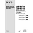
 $4.99 CSDFD92 AIWA
Owner's Manual Complete owner's manual in digital format. The manual will be available for download as PDF file aft…
|
|
 |
> |
|
