|
|
|
Who's Online
There currently are 6043 guests online. |
|
Categories
|
|
Information
|
|
Featured Product
|
|
|
 |
|
|
There are currently no product reviews.
 ;
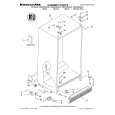
Some of the pictures in this manual are a bit irritating. I had to dissassemble the unit and some of the screws have different threads, which is not mentioned in this manual. Also some of the drawings of the boards look different than the actual boards.
After all, the manual was very useful. I was able to recalibrate the capstan drive and it is working fine again.
 ;
This manual is very good. 303 pages scanned in a very high resolution. My camera has bad, leaking capacitors which all of the V5000 models are suffering from these days.
There is a huge part list with all capacitors, transistors etc. in this manual which helped me a lot. Otherwise I would not have been able to buy replacement parts.
The dissassembly guide is very enormous and detailed. Unlike on the Panasonic MS1 manual I downloaded here it actually looks like the real parts look. And the screws are labeled correctly, so you shouldn't have any left after the repair. ;)
;
has all the schematics you could need,and very well laid out format also has all part numbers along with an exploded view which is helpful
;
Very nice to have! Now it is no problem to understand how it is put together.
Helps me a lot.
;
good scans, all is clear. all pages in order. recommended
CD SECTION
Note: 1. CD Block is basically designed to operate without adjustment. Therefore, check each item in order given. 2. Use YEDS-18 disc (3-702-101-01) unless otherwise indicated. 3. Use an oscilloscope with more than 10 M� impedance. 4. Clean the object lens by an applicator with neutral detergent when the signal level is low than specified value with the following checks.
E-F Balance (1 Track Jump) Check
oscilloscope BD board TP (TE) TP (VC)
+ �
VIDEO SECTION Frequency Adjustment
Connection:
frequency counter VIDEO board (27 MHz) + �
S-Curve Check
oscilloscope BD board TP (FE) TP (VC)
+ �
Procedure : 1. Connect oscilloscpe to TP (TE) and TP (VC). 2. Turn the power ON. 3. Load a disc (YEDS-18) and playback the number five track. 4. Press the ^ (CD) button. (Becomes the 1 track jump mode) 5. Confirm that the level B and A (DC voltage) on the oscilloscope waveform.
1 track jump waveform
Procedure: 1. Connect oscilloscope to TP (FE). Connect between TP (FE1) and TP (VC) by lead wire. Connect between TP (AGCCON) and TP (GND) by lead wire. Turn the power ON. Load a disc (YEDS-18) and actuate the focus search. (In consequence of open and close the disc tray, actuate the focus search) 6. Cofirm that the oscilloscope waveform (S-curve) is symmetrical between A and B. And confirm peak to peak level within 4 ± 1 Vp-p.
S-curve waveform
symmetry
2. 3. 4. 5.
center of waveform B
Procedure: 1. Connect the frequency counter to check point of the VIDEO board. 2. Turned power switch on. 3. Press the FUNCTION button to select the CD. 4. Adjust CT503 on the VIDEO board so that the frequency counter reading 27.0 MHz ± 80 Hz at stop status. Adjustment Location:
0V
A (DC voltage)
VIDEO Board (SIDE B)
level = 1.3 ± 0.6 Vp-p
symmetry
A Specified level: B � 100 = less than ± 22%
6. After check, remove the lead wire connected in step 1.
A within 4 ± 1 Vp-p B
Checking Location: BD BOARD (Side B)
CN501
100 81 51 80 SL501 SL502
TP (FE1)
7. After check, remove the lead wire connected in step 2 and 3.
Note: � Try to measure several times to make sure than the ratio of A : B or B : A is more than 10 : 7. � Take sweep time as long as possible and light up the brightness to obtain best waveform.
(GND) 30
TP (AGCCON) TP (GND) TP (RF)
1
RF Level Check
oscilloscope BD board TP (RF) TP (VC) + � IC102 TP (TE) TP (FE) IC103
CT503 31 VIDEO Frequency Check point Adjustment (27 MHz) 50
IC505
Procedure: 1. Connect oscilloscope to TP (RF). 2. Connect between TP (AGCCON) and TP (GND) by lead wire. 3. Turn the power ON. 4. Load a disc (YEDS-18) and press the ^ button to play. 5. Confirm that the oscilloscope waveform is clear and check RF signal level is correct or not. 6. After check, remove the lead wire connected in step 2.
Note: Clear RF signal waveform means that the shape ��� can be clearly distinguished at the center of the waveform.
CN502
IC101 TP (VC)
D502
SL503
VOLT/DIV: 200 mV TIME/DIV: 500 ns
level: 1.45 ± 0.3 Vp-p
17
17
|
|
|
> |
|