|
|
|
Categories
|
|
Information
|
|
Featured Product
|
|
|
 |
|
|
There are currently no product reviews.
 ;
buen manual con sus formas de onda y esquemas , completo y de buena calidad de imagen, es correcto.
 ;
This is exactly what I needed This was a hard one to find and I had already downloaded several for other Panasonic radios but none matched my radio.
Although my radio is the LBE model the LBS is the same.
A very good quality manual with every thing you should get in it
 ;
el manual es correcto , completo y de buena calidad aunque algun esquema esta excesivamente diseccionado.
 ;
muy buen manual con multiples graficos y formas de onda ademas de muy completo y bien presentado.
 ;
As Always these people were very rapid and efficient. A great job helping hobbiest and workers!!! Thank you a lot!
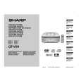
QT-V5E/QT-V5H
E Market Service QT-V5E/QT-V5H Audio Manual CHAPTER 6. OTHERS [1] Function table of IC
IC101 9HX06526160501: PLL (BU2616F) Pin No. 1 2 3 4 5 6 7 8 9 10 11 12 13 14 15 16 17 18 Terminal Name XOUT XIN CE DA CK DO SD IFIN P3 P0 P1 P2 AMIN FMIN VDD PD1 PD2 VSS Input/Output OUTPUT INPUT INPUT INPUT INPUT �� INPUT INPUT �� �� �� �� INPUT INPUT INPUT �� �� �� Setting in Reset Crystal oscillation Crystal oscillation Chip enable Serial data Clock signal Data out SD input IF input OUTPUT Function For generation of standard frequency and internal clock. Connected to 7.2 MHz crystal resonator. When CE is H, DA is synchronous with the rise of CK and read to the internal shift register. DA is then latched at the timing of the fall of CE. Also, output data is output from the CD terminal synchronous to the rise. Comes ON during IF frequency detection or SD detection. SD signal is input, Observed by DO terminal. Input is for IF frequency. Controlled on the basis of input.
AM input FM input Power supply Phase comparison output GROUND
Local input for AM. Local input for AM. Power supply, with 4.0 V to 6.0 V applied voltage. High level when value obtained by dividing local output is higher than standard frequency. Low level when value is lower. High impedance when value is same. GROUND
IC203 9HX06830480284: DC-DC Converter (IRU3048CS) Pin No. 1 2 3 4 5 Terminal Name GND FB2 COMP1 COMP2 VCH2 Function Ground pin. Inverting inputs to the error amplifiers. These pins work as feedback inputs for each channel, and are connected directly to the output of the switching regulator via a resistor divider to set the output voltages. Compensation pins for the error amplifiers. Compensation pins for the error amplifiers. Supply voltage for the high side output drivers. These are connected to voltages that must be at least 4 v higher than their bus voltages (assuming 5 v threshold MOSFET). A minimum of 1µF high frequency capacitor must be connected from these pins to PGng pin to provide peak drive current capability. Output driver for the high side power MOSFET. Connect a diode, such as BAT54 or 1N4148, from these pins to ground for the application when the inductor current goes negative (Source/Sink), soft-start at no load and for the fast load transient from full load to no load. Output driver for the synchronous power MOSFET. This pin serves as the separate ground for MOSFET�s driver and should be connected to the system�s ground plane. Supply voltage for the internal blocks of the IC. Output driver for the synchronous power MOSFET. Output driver for the high side power MOSFET. Connect a diode, such as BAT54 or 1N4148, from these pins to ground for the application when the inductor current goes negative (Source/Sink), soft-start at no load and for the fast load transient from full load to no load. Supply voltage for the high side output drivers. These are connected to voltages that must be at least 4 v higher than their bus voltages (assuming 5 v threshold MOSFET). A minimum of 1µF high frequency capacitor must be connected from these pins to PGng pin to provide peak drive current capability. Driver signal for the LDO�s external transistor. LDO�s feedback pin, connected to a resistor divider to set the output voltage of LDO. Soft-Start pin. THE converter can be shutdown by pulling this pin below 0.5 v. Inverting inputs to the error amplifiers. These pins work as feedback inputs for each channel, and are connected directly to the output of the switching regulator via a resistor divider to set the output voltages.
6
HDRV2
7 8 9 10 11
LDRV2 PGND VCC LDRV1 HDRV1
12
VCH1
13 14 15 16
VOUT3 FB3 SS FB1
6�1
 $4.99 QTV5H SHARP
Owner's Manual Complete owner's manual in digital format. The manual will be available for download as PDF file aft…
|
|
 |
> |
|
